Reason about the technology
Relate layers, device models and design rules to the educational or licensed PDK selected for the program.


Connect first principles to the decisions behind a working circuit. Cloud Campus brings a learning management system (LMS), courses and pathways together with hands-on semiconductor design and verification in WCS.
Learn why a circuit behaves as it does, test your reasoning and explain the result.

One integrated learning environment
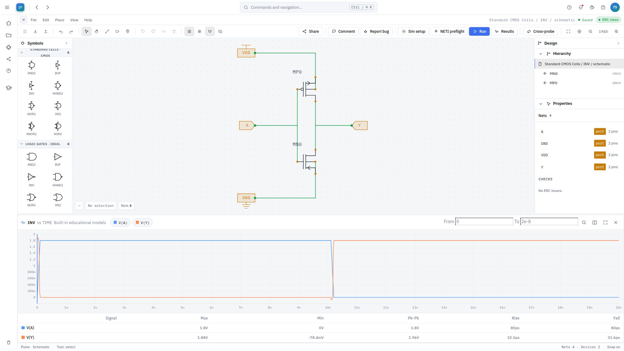
Follow a concept into schematic, simulation and layout work. The course gives the explanation; the WCS tools give learners a way to investigate it.
Predict how the output responds to an input. Build the circuit, run a simulation and explain the waveform. Then connect the circuit to its physical implementation.
A pathway to deeper understanding
Choose a structured pathway or an individual course. Progress from semiconductor fundamentals to richer design, verification and research questions.
Curriculum preview. Course availability and prerequisites are agreed for each program.
Explore layers and connectivity, then follow a guided CMOS inverter project.
Build a CMOS cell, investigate its behaviour and work through DRC and LVS checks.
Bring schematic, simulation, layout and verification together in an end-to-end capstone.
Investigate richer design constraints and develop a design and verification capstone.
Frame a research question, explore a circuit and explain the results of the investigation.
Develop the habits behind reliable design
Connect electrical behaviour to physical implementation. Hands-on exposure to PDKs, DRC and LVS helps learners understand why a design passes a check, why it fails and what to investigate next.
Relate layers, device models and design rules to the educational or licensed PDK selected for the program.
Inspect highlighted DRC findings in the layout. Investigate opens, shorts and connectivity mismatches through LVS.
Ask NETI AI about supported findings or results, open the cited source and test the explanation in the tools.
Meet NETI AIFor classrooms and engineering teams
Combine self-paced study with instructor-led learning, project reviews and capstones. Shape the program around your learners and teaching goals.
Connect coursework to design labs and capstones. Use learner progress and assignment review to guide the next teaching conversation.
Build a focused program for onboarding or deeper circuit, layout and verification knowledge, with practical exercises your team can discuss.
Bring your learning goals
Walk through the learner experience with your faculty, students or engineering team.